The first and seemingly most important step is to ensure that the Product Development Kit (PDK) is fine tuned and well supported. IE: Device level placements will be made accurately the first time if auto cell abutment “Servers” are working properly. Another example of the importance of PDK development and use is routing. Any senior level custom analog designer knows well, a double cut VIA can make all the difference between a working circuit and not. Yet achieving that goal can lead to significantly more design time.
The initial focus should be Device Placement requirements like matching or mirroring. Both custom Analog and Digital circuits must have initial ideas established for device placements. Floor planning should always begin at the highest level possible. It seems that 90% of rework gets performed because this activity was not performed. Initial placement ideas should be followed by identifying pin location constraints as they effect device placement locations. Next, the nWell, pWell and any isolation scheme must then be established. Bulk connections (or back gates or gate ties) must be accounted for. Finally, dummies need to be instantiated and preferably accounted for in the schematics.
Device Placement
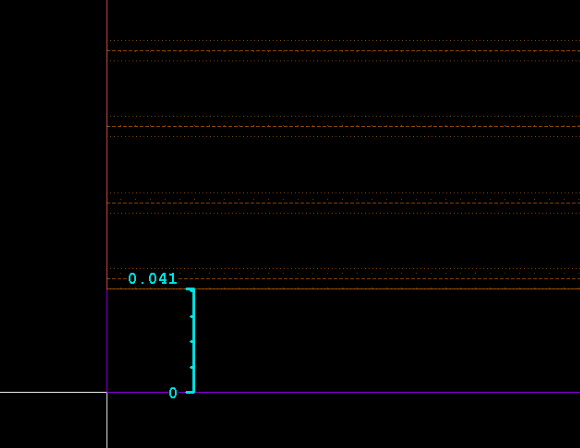
When inital placements are made, before running DRC verification, the designer must ensure all diffusion (OD) be placed on the default 30nm (0.030) fin grid. See picture 1. The quickest and most efficient way to ensure fin grid alignment during placement starts with the prBoundary.boundary layer placement. The lower left corner of this should be placed at origin 0 0. Next, the finBound.fb1 should be drawn. Left and right sides of the finBound.fb1 should be adjacent to the prBoundary.drawing layer. Top and bottom of finBound.fb1 layer must be inside the prBoundary.boundary layer exactly 41nm (0.041). See picture 2. Finally, move the OD objects so that they align horizontally with the finBound.fb1 layer. See picture 3.
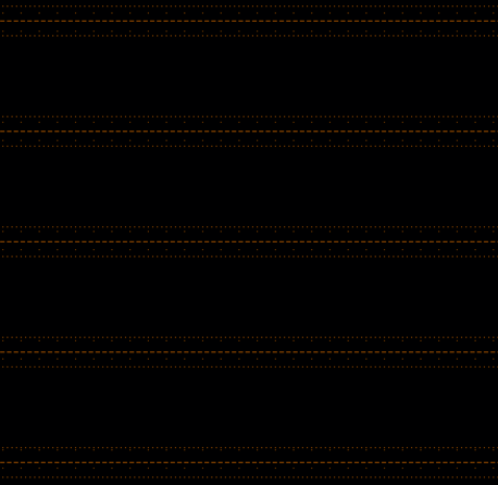 Fin Grid . Where the fins appear during process.
Diffusion and Dummy Diffusion placed properly on the fin grid.
When placing these finFet pCells a Virtuoso Cad Designer is in a 2d world. They will not see the “Fins” on the devices. Unlike regular mosfet devices, which have “Source, Gate & Drain” laid out sort of perpendicularly, finFet pCells connect parallel. So while placements are being made, Source, Gate and Drain positions must be considered carefully.
With all of these concepts well understood the initial device placement can proceed. It is imperative the design block be verified through DRC before main routing takes place. Issues such as density are extremely complex and require much adjustment to the base layers. It should be of great concern if the cell is too small for density windows and therefore will not show any issues. That is until that cell is used at another level up. Some of these density issues had to be corrected and extensive re-work was required.
Furthermore, in every case from my experience, no matter how simple the block appeared (IE: Simple Level Shifter), odds are high that unaccounted for DRC errors will occur. Since the average DRC runs uses over 7000 rules on every cell, one would expect this to happen. As discussed above, there are many forms of density violations and all should be considered.
IE: I had a block with many 8nm devices all brought together. Since 8nm size requires at least 2 microns worth of strips horizontally and 36 square microns minimum area, those density errors do require attention and will not be “Fixable” further up the hierarchy using density fill tools. In another example, I aligned devices along the poly array and utilized the layer “CPO” (cut poly). That way the poly stripes could stay in place and not short out with each other. This worked great until the next level up where not so much CPO was used in the other blocks. This caused a gradient error DRC showing to be over maximum CPO density rules. Once again, lower level rework had to be performed. Absolute bottom line is density violations must be considered it great detail.
Routing
Once placement DRC is complete, routing can be performed. Within the following paragraphs there are core concepts which must be considered before routing begins.
The mask designer should perform a DRC check after any large route or large group of routes have been created. Just like with device placement, possibilities for unaccounted DRC error issues exponentially grow with every connection made.
All metal objects must be rectangular. No exceptions. These rectangular objects are limited in width and sometimes required to be set on a grid designated for that metal. IE: Metal 1 widths can only be 20nm, 60nm, 76nm, 110nm, 120nm and 180nm. Any other widths are not allowed.
In order to connect metal to deep sub micron devices, lower level metals (M0, M1, M2, M3 typically) must have “Mask A” or “Mask B” color properties. When a wire gets laid out (created) for any type of semiconductor, a bleeding effect occurs causing jagged edges. With large width metals this does not really matter much. But when the required widths get small enough, this jagged edge really matters. These are corrected through an etching step which clears the way for another metal of the same like to be laid down next to and in parallel. It should be noted that the mask 2 is slightly less resistive than mask 1. The physical design teams actually utilize this in order to alleviate start and stop time errors.
While creating routes, the mask designer designates (assigns) and locks colors to the rectangular metal objects (and vias) representing metal mask “A” or metal mask “B”. Every object requires a locked mask color designation. Once these color’s become established and locked the DRC rules will allow for significantly close like metal lines. IE: A mask designer has 2 Parallel 20nm metal1 lines run from one place to another in their circuit ( about 1 micron). The minimum space between these metal1 lines if they were the same mask color would be 120nm. If one of those lines are designated and locked as “MaskA” (or highlighted in dark red) and the other parallel 20nm line is designated and locked as “MaskB” (or highlighted in dark green), minimum space requirement would drop significantly.
With this process you can use square and rectangular VIA’s to best optimize your connections. That helps, but the MD needs to create cut layers which initially meet DRC requirements which are extensive. Routing lower level metals with multiple mask options creates a 2 way perspective on metal spacing’s and via enclosures.
Completion
If the mask designer utilizes Cadence Virtuoso XL specialized tool “Annotation Brower” combined with “Layout Extraction” then LVS stage will have minimum issues. When utilizing layout extraction it is important to remember that pCells and instantiated macro’s can lose their true connectivity.
If the PDK works, is well supported and the mask designer utilizes these notes and instructions, productivity will be maximized.
